 网站首页
网站首页
 购物车
购物车 用户中心
用户中心 全部产品分类


服务热线
4006988696
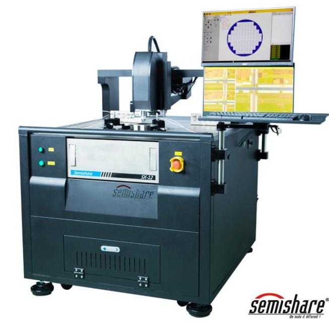
基于公司技术团队在半导体光电子材料及器件领域十多年的技术积累以及MOCVD、EBL、ICP等专业设备平台,为企业、高校、科研院所提供半导体光电外延片材料的全方位代工服务,涵盖光电外延片结构设计、材料外延、光栅制作、测试分析等方面,主要服务内容包括InP基材料和器件(LD/PD/QPSK/Modulator)、GaAs基材料和器件(LD/Solar Cell/SESAM/PD)、GaSb基材料和器件(LD/PD/SESAM)、GaAs和InP基量子点材料和器件、硅基III-V材料和器件(Heteroepitaxy)等。
| 分类/Category | 应用/Application | 说明/Description |
| 光电材料外延和表征 Customer designed epitaxy & characterization |
GaAs/InP based bulk/quantum well/quantum dot Superlattice/tunnel junction |
|
| GaAs/InP based secondary epitaxy | P or N-doped InGaAs/InP, AlGaAs/GaAs | |
| Butt-joint regrowth | InGaAsP/InP | |
| Holographic grating fabrication | ||
| Designed nano-pattern (grating/nano-hole) fabrication by Electron Beam Lithography | ||
| XRD/PL mapping/Hall/ECV/SEM | PL detector (800-2400 nm) |
商家资料
提示:注册 查看!
